Home > Products >> Custom Optics and Sub-Assembly
Custom Optics and Sub-Assembly
Vertical Rotary Surface Grinders - designed to flat grind a wide variety
of optical and crystalline materials to tool room accuracy and surface
finish. All bearings and critical components are shielded from abrasive
and liquid contaminates. Infinitely variable stepless infeeds eliminates
chipping and sub-surface fracturing.
Lens Centering/Beveling -- Bell Clamp Lens Centering Machine, 1 - 90
mm diameter work capacity.
Lens Curve Generation - This lens curve generator can generate high precision
spherical curves on all lenses up to 120 mm diameter. Lens chuck seats
are cut on the spindles, increasing overall accuracy.
Lens Cementing - This self-contained workstation is equipped to handle
a variety of lens cementing and inspection or cleaning applications.
Core Drilling - Our core drilling equipment can drill holes which are
perpendicular or at an angle to the surface of the element, in glass,
metals and ceramic materials.
Shaping - We have various CNC machine able to produce intricate configurations
on various meterials.
Optical Sub-Assembly
Custom Optical Sub-Assembly help customer:
• Minimize optic handling & reduce the risks such as damage and
contamination
Our engineering staff is experienced in the manufacturing techniques
that produce repeatable and dependable products. We fabricate optical
components, design thin film coating, design unique mount and assembly
procedures. Optical sub-assemblies are are performed in Class 10,000 clean
rooms and on Class 1,000 Laminar Flow benches, ensuring that our customers
receive high quality products every time.
Optical Contact Bonding
Optical contact bonding is a glueless process whereby two closely conformal
surfaces are joined together, being held purely by intermolecular forces.
Optical contacting is used in the manufacture of micro-optic systems for
a variety of applications from biophotonics to telecommunications.
Key Features
- Adhesive-free bonding of coated or uncoated surfaces
Micro-optic systems consisting of prisms, beamsplitters and other optical
components are used across a variety of industries from telecommunications
to biophotonics. They can increase the efficiency of fiberoptic and endoscopic
imaging systems in medical and biophotonic applications, lock the wavelength
of telecommunications transmitters, or increase the lasing efficiency
in high-power lasers. The optics in these microsystems are bonded together
so that no extra fixturing is required. A variety of processes such as
epoxy bonding, frit bonding, diffusion bonding, and optical contacting
have been used. The quality of the bond and interface is judged on several
criteria, including precision, mechanical strength, optical properties
(scattering, absorption, index mismatch, and power handling), thermal
properties, and chemical properties, along with the simplicity and
manufacturability of the process itself.
Epoxy Bonding
One of the most common methods used to adhere two pieces of optical glass
is epoxy bonding. The two pieces are coated with epoxy, brought together,
and cured (time, temperature, or UV exposure). Epoxy bonding is reliable
and manufacturable because it is an inexpensive process with high yield.
However, because it leaves an often thick and variable film, it is inappropriate
for applications requiring precision thickness control. Scattering can
occur in these optically thick interfaces, introducing loss. And, because
the epoxy is often made from organic material, these bonds cannot withstand
high-intensity optical powers or UV exposure. Moreover, epoxy bonds are
not particularly heat resistant or chemically robust. Because the pieces
are “floating” on a sea of epoxy, they can move under various
thermal conditions. The epoxy can also dissolve with chemical exposure.
In a vacuum environment, the epoxy can outgas and contaminate other optics.
For these reasons, there is great interest in epoxy-free bonding technologies.
Frit Bonding
Frit bonding, a process that uses a low-melting-point glass frit as an
intermediate bonding agent, is widely used for both optical and MEMs applications.
It is an epoxy-free process in which the substrates are polished, cleaned,
and coated with a glass frit. The pieces are baked together at high temperatures
(in the range of 400°C to 650°C) and with moderate pressure. The
benefit is that the bond is mechanically strong and chemically resistant.
There are several drawbacks, however. Because the melted glass frit bonds
the parts together, the frit must be able to flow between the parts. In
some cases, the parts must be grooved to enable the frit to flow evenly,
increasing scattering in the final interface. Moreover, the process is
expensive because the fixtures must withstand extremely high temperatures.
Also, these high temperatures can cause changes in the physical and chemical
properties of the materials themselves, including changes in dopant concentrations
and/or structural changes.
Diffusion Bonding
Another epoxy-free bonding process is diffusion bonding, first developed
as a cost-effective method for the fabrication of titanium structural
fittings (instead of costly machining) for military aircraft systems including
the B-1 bomber and the Space Shuttle. In this process, the two optical
pieces are heated and then pressed together. Because the bonding process
relies on the atomic diffusion of elements at the interface, the required
temperature can be up to 80% of the melting temperature of the substrates
themselves (often greater than 1000°C).The atoms migrate through the
solid, either by the exchange of adjacent atoms, the motion of interstitial
atoms, or the motion of vacancies in the lattice structure; the two glass,
ceramic, or metal substrates must be in very close proximity for the diffusion
process to take place. Initial surface flatness and cleanliness are essential.
Because the material is heated up, expensive fixturing is required, and
chemical changes can occur (dopant concentrations can be altered).
Optical Contacting
Optical contacting is a room-temperature bonding process that results
in an epoxy-free precision bond. The process results in optical paths
that are 100% optically transparent with negligible scattering and absorptive
losses at the interfaces. In traditional optical contacting, the surfaces
are polished, cleaned, and bonded together with no epoxies or cements
and no mechanical attachments.
The technique has a long history-the adhesion of solids was first observed
two centuries ago, when Desagulier in 1792 first demonstrated the bonding
of two spheres of lead when pressed together.1 Because the sphere deformed
in the process, this could not be used for rigid materials such as quartz
and fused silica. About a century ago, German craftsmen used the technique
“ansprengen” (meaning “jumping into contact”) to stick
together two optically polished bulk pieces of metals for precision measurements.
They used an analogous method with optically polished glasses for making
precision prisms. Nonetheless, it was not until 1936 that a systematic
investigation took place with Lord Rayleigh’s studies of the room-temperature
adhesion mechanism between two optically polished glass plates.
Optical contacting has been used for years in precision optical shops
to block optics for polishing because it removes the dimensional uncertainty
of wax or adhesives. Because the process is not very robust and can be
easily “broken,” parts optically contacted in the traditional
manner must be sealed around the edges to prevent breaking the contact.
Today, however, variations on traditional optical contacting can create
precise, optically transparent bonds that are robust and mechanically
strong. These improved processes result in a bond as strong as if the
entire structure had been made from a single piece of material, and bonds
have even passed Telcordia’s stringent requirements for durability,
reliability, and environmental stability. Because these bonds are epoxy-free,
they can withstand high optical powers and low temperatures. There is
no scattering or absorptive losses at the interfaces and no outgassing.
The bond is chemically resistant and can be used with a wide variety of
materials; both similar and dissimilar crystals and glasses can be bonded.
Modern day uses of improved optical contacting include composite high-power
laser optics (structures that have a doped “core” with a different
cladding material), micro-optics, cryogenic optics, space optics, underwater
optics, vacuum optics, and biocompatible optics.
Almost all these improved optical-contacting processes use a variation
of “wafer bonding”-analogous to a similar process in the semiconductor
industry. These processes include an extra step to create covalent bonds
across the interface-a bond that is significantly stronger than that formed
from traditional optical contacting. This extra step can be increased
pressure, chemical activation, and/or thermal curing.
For example, one solution-assisted process uses an alcohol-based optical
cleaning solution (isopropyl alcohol or similar) so the parts can be aligned
before the alcohol evaporates.3 This facilitates alignment of the optical
components and eliminates one disadvantage of conventional optical contacting:
it is difficult or impossible to adjust the alignment once the components
have bonded. The solution forms a weak bond that strengthens as the alcohol
evaporates, typically about one minute. While this solution-assisted process
addresses the alignment issue, there are still tight requirements on the
flatness and cleanliness of the pieces.
Chemically Activated Direct Bonding
Another epoxy-free solution-assisted optical-contacting process is chemically
activated direct bonding (CADB). Developed by Precision Photonics, it
is a highly repeatable and manufacturable process that relies on a well-studied
chemical activation. The process results in a bond as strong as bulk material,
as precise and transparent as traditional optical-contact bonds, and as
reliable as high-temperature frit bonding. Most important, it can be performed
with high yields with a variety of materials, including dissimilar materials,
and over large areas.
With traditional optical contacting, bonds over large areas are often
difficult because of surface irregularities. Today's modified solution-assisted
processes relax the incoming requirements, enabling optical-contact bonding
over large areas without any voids.
In CADB, the parts are polished and physical and chemical contaminants
removed. The surfaces are chemically activated to create dangling bonds.
The two parts to be bonded are brought into contact with each other, at
which point the outer molecules from each surface bond together through
hydrogen bonding. The parts are then annealed at a temperature specific
to the substrate materials. During annealing (at temperatures well below
melting temperatures), covalent bonds are formed between the atoms of
each surface, often through an oxygen atom. CADB has been successfully
used for a variety of applications, including composite bonding of dissimilar
materials, in which it is typically only limited by the mismatch of the
coefficient of thermal expansion of the materials. Material combinations
successfully bonded together include YAG/sapphire, quartz/BK7, and fused
silica/Zerodur.
Chemically activated direct bonding can also be used to bond coated materials.
Ion-beam-sputtered (IBS) and ion-assisted coatings are hardy enough to
withstand the bonding process. A repeatable and controllable high-energy
process, IBS results in dense, durable dielectric thin films. Because
the molecules in the IBS process are deposited at a high average energy
(unlike evaporative or ion-assisted processes that are low energy), the
molecules form covalent bonds. The resulting films are extremely uniform
and nonporous and offer superior adhesion. The deposited molecules in
the IBS process have energies of approximately 10 eV, or 100 times their
thermal energies.
Since it was first observed more than 200 years ago, optical contacting
has evolved from a “black art” to a highly manufacturable and
repeatable process used in the manufacture of a variety of components.
Today’s optical-contacting methods offer increased robustness and
flexibility when compared to traditional optical contacting. For example,
CADB can bond a variety of crystal, glass, and ceramic materials (such
as fused silica, LaSFN9, Zerodur, BK7, ULE, YAG, ceramic YAG, sapphire,
YVO4, and doped phosphate glasses), and can also be used over large areas
for high-volume applications, even on ion-beam-sputtered and ion-assisted
dielectric thin films.
Diffusion bonding of strongly anisotropic double tungstate crystals with
high quality interfaces was successfully implemented. The bonded Yb:KY(WO4)2/KY(WO4)2
composite crystals showed an impressive performance both in the continuous-wave
and mode-locked laser regime. More than 800 mW of continuous-wave output
power at 1.04 µm and slope efficiencies up to 70% were obtained
at room temperature without cooling. In the passively mode-locked regime,
pulse durations as short as 66 and 62 fs have been achieved directly from
the oscillator and with external compression, respectively. ©2008
The Japan Society of Applied Physics
Epoxy-free Products and Components:
- Microchip and Thin disk lasers
Optical and Optoelectronic Assembly Service
Optical assembly and optoelectronic assembly services design assemblies
and systems for optical and optoelectronic devices. They provide optical
assembly and optoelectronic interfacing between devices, facilitate optical
and optoelectronic data transfers across networks, and provide optical
and optoelectronic packaging of active and passive components with different
optical properties, materials, shapes and sizes. In many optoelectronic
systems, electrical and optical inputs/outputs (I/O) must be packaging
together in order to provide electrical-to-optical and optical-to-electrical
conversion. High-resolution optical encoders are used with servo-controlled,
direct-drive brushless DC motors. Optical switches are used to provide
network connectivity through a series of micro-electrical-mechanical-system
(MEMS) mirrors and lenses that direct light between I/O fibers.
Optical assembly and optoelectronic assembly services perform processes
such as metallization, soldering, alignment and sealing. Hermeticity or
air tightness is an important consideration because of the sensitivity
of optical and optoelectronic devices. Contaminants can scratch the lenses
in optical equipment and obstruct optical-to-electrical communication
pathways. Consequently, optical assembly and optoelectronic assembly services
maintain cleanroom-type environments and follow strict production procedures.
Inspectors who work for optical and optoelectronic assembly services use
optical instruments such as spectrometers, polarimeters and photometers
to identify defects. In many cases, an optical assembly service or optoelectronic
assembly service may also manufacture semiconductors, integrated circuits
(IC), printed circuit boards (PCBs) or other components that require high-purity
conditions.
Optical assembly and optoelectronic assembly services are certified by
the International Standards Organization (ISO) and/or the IPC, a trade
association formerly known as the Institute for Interconnecting and Packaging
Electronic Circuits. ISO 9001:2000 certification is a part of the larger
ISO 9000 standard. It contains the actual requirements with which optical
assembly services and optoelectronic assembly services must comply. IPC-A-610
certification is often required for inspectors, manufacturing personnel,
and other employees of optical and optoelectronic assembly services who
examine products for defects.
Custom Optics and Sub-Assembly Inquiry
☃
sales@optocity.com.
©2017 www.optocity.com ---Back^^Top
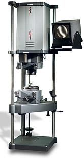 OptoCity provide a full optical fabrication facility to meet your precison
optical requirements. We fabricate a vast range of custom and stock precision
optical components from the widest variety of materials: Crystal, Glass,
Transparent ceramic, Optical plastic, etc. We can also work with materials
supplied by the customer.
OptoCity provide a full optical fabrication facility to meet your precison
optical requirements. We fabricate a vast range of custom and stock precision
optical components from the widest variety of materials: Crystal, Glass,
Transparent ceramic, Optical plastic, etc. We can also work with materials
supplied by the customer.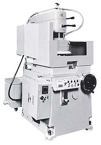 Conventional
grinding & polishing machines - varying sizes and work capacities
offering efficient and economical polishing of all optical glasses.
Conventional
grinding & polishing machines - varying sizes and work capacities
offering efficient and economical polishing of all optical glasses.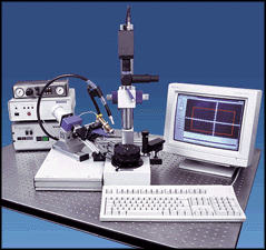 Optical Bonding Station - The Automatic Cementing and Bonding Station
extends its capabilites
into the production process of optical components and systems. This Bonding
Station includes all the devices necessary for accurate and automated
work: cement dispensers, stepper motor positioning unit for dispenser
needle, UV-curing lamp, rotary position sensing device, multi-task PC-processing
card and a main controller unit.
Optical Bonding Station - The Automatic Cementing and Bonding Station
extends its capabilites
into the production process of optical components and systems. This Bonding
Station includes all the devices necessary for accurate and automated
work: cement dispensers, stepper motor positioning unit for dispenser
needle, UV-curing lamp, rotary position sensing device, multi-task PC-processing
card and a main controller unit.